Contents
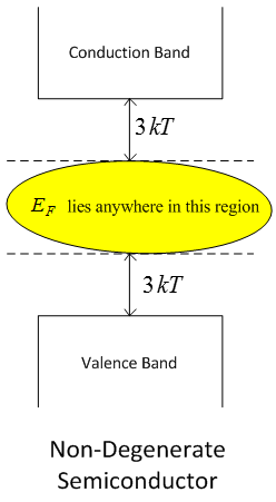
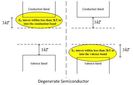
Degenerate & Non-Degenerate Semiconductor
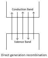
Direct Generation & Recombination
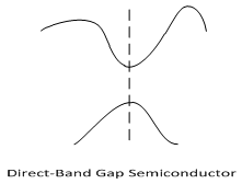
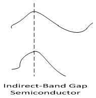
Direct/ Indirect Band Gap Semiconductor
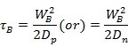
Fabrication of a planar JN Diode
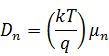
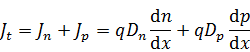
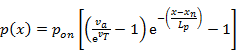
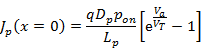
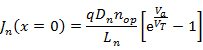
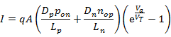
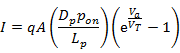
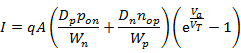
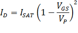
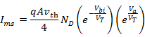
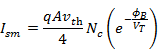
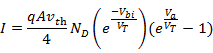
Shockley's Equation for Drain Current
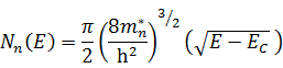
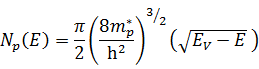
· The densities of electrons and holes in the conduction and valence bands depend on two factors
1. Density of states available for occupancy (given by N(E)).
2. Probability of occupancy of states (given Fermi function).
· Density of states
·
![]()
· Fermi Function
·
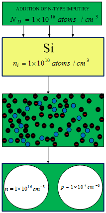
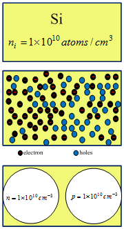
There are about ![]() atoms/cm3 in
silicon. At T=0K, the 4N quantum states in the valence
atoms/cm3 in
silicon. At T=0K, the 4N quantum states in the valence
band are filled with electrons and the 4N states in the conduction band are empty. Ec and Ev represent the maximum electron energy in the conduction band and maximum hole energy
in the valence band respective.
· To simplify integration Boltzmann approximation is introduced and the unity is dropped from Fermi function.
· Boltzmann approximation is restricted to the range of Fermi energies extending from 3kT above the top of the valence band and 3kT below the bottom of the conduction band. Based on this classification we have generate and non-degenerate semiconductors.
|
P-type impurity |
N-type impurity |
|
Boron |
Phosphorous |
|
Aluminum |
Arsenic |
|
Gallium |
Antimony |
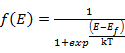
· FERMI-DIRAC FUNCTION functions give the probability that an electron occupies a quantum state with energy E.

|
Densities of state in the conduction band |
|
|
||||||||
|
Densities of state in the valence band |
|
|
||||||||
|
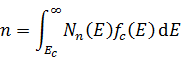
Density of electrons in the conduction band |
|
|
||||||||
|
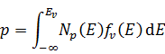
Density of holes in the valence band |
|
|
||||||||
|
Intrinsic carrier density |
|
·
·
decreases
with increase in |
||||||||
|
Charge neutrality |
|
|
||||||||
|
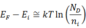
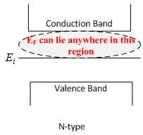
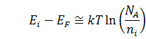
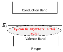
Location of Fermi level in n-type and p-type
For intrinsic semiconductors
|
|
|
|
|
|
|
P-type impurity |
N-type impurity |
|
Boron |
Phosphorous |
|
Aluminum |
Arsenic |
|
Gallium |
Antimony |
|
Semiconductor |
Energy Gap (eV) |
|
Ge |
0.67 eV |
|
Si |
1.12 eV |
|
GaAs |
1.42 eV |
|
|
|
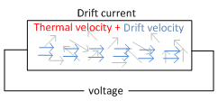
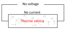
· Thermal velocity does not result in current.
· Drift velocity results in drift current.
· Drift velocity is much smaller in magnitude than thermal velocity.
· Drift velocity does not increase with increase in electric field because of scattering.
· Scattering occurs because of the following:
1. Lattice vibration (effective at high temperature).
2. Presence of ionized impurity (effective at low temperature).
· It is also known as Impurity scattering.
3. Lattice imperfection
·
Scattering is represented by scattering time ![]() (the
time between two successive collisions)
(the
time between two successive collisions)
|
Drift Current |
|
|
|
Drift velocity of electrons |
|
It is of the
order |
|
Drift velocity of holes |
|
|
|
Mobility & Drift velocity |
|
|
|
Mobility (electrons) |
|
Dimension [ |
|
Mobility (holes) |
|
|
|
Conductivity (due to holes) |
|
|
|
Conductivity (due to electrons) |
|
|
|
Total conductivity |
|
|
|
Total resistivity |
|
|
|
Total drift current density |
|
|
|
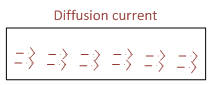
Diffusion current due to electrons |
|
Dimension |
|
Diffusion current due to holes |
|
|
|
Diffusion current |
|
|
|
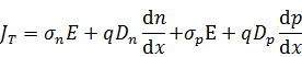
Total current density |
|
|


Causes of Direct-generation of electron-hole pairs:
1. Exposure to thermal energy.
2. Exposure to light energy.
3. Impact ionization.
Cause of Indirect-generation of electron-hole pairs:
1. Lattice imperfection
|
|
· Traps=Gold & Iron in silicon and Copper in Ge. · Recombination-generation occurs through traps.
|
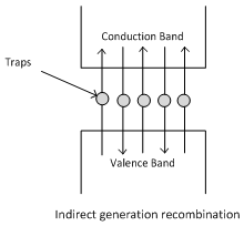
· Expression for rate of change of carrier density with time for indirect-generation-recombination
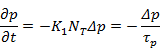
![]()
· Low Level Injection: Any perturbation such that the change in minority carrier density is much smaller than the majority carrier density is called a low-level injection.
· Most devices work in this condition when excess minority carriers are injected.
· Change in majority carrier density is so small that it is considered constant.
|
Eg: GaAs |
Eg: Si & Ge |
· Equation of continuity
![]() for holes in the N-region
for holes in the N-region
![]() for electrons in the P-region
for electrons in the P-region
· Haynes Shockley Experiment gives:
1. Lifetime of minority carriers.
2. Mobility.
3. Diffusion constant.
· Hall's Effect experiment gives:
1. Carrier concentration.
2. Type of the semiconductor.
|
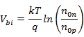
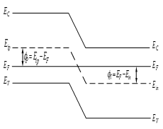
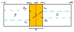
Barrier Potential |
|
|
|
Constancy of Fermi Level |
|
|
|
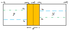
Electrostatic in the space Charge region |
|
|
|
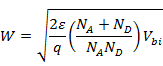
Width of the space charge region |
|
|
|
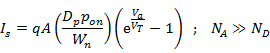
Diffusion current (with bias voltage) |
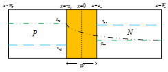
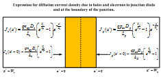
Carrier density of holes and electrons in the n-region and
p-region respectively for
Diffusion current density at the boundary
Current in the
diode at the space charge boundary for (
If
Current in the
diode at the space charge boundary for (
|
|
|
Diffusion current in the diode (at equilibrium) |
The magnitude of diffusion current at equilibrium is much larger than that at forward bias. |
|

|
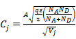
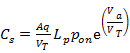
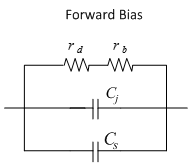
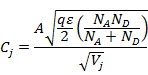
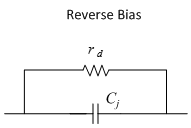
Capacitance
1. Transition Capacitance. 2. Diffusion (Storage)Capacitance. |
· Transition capacitance exists in both forward and reverse bias. · It is due to the accumulation of ions in the depletion region. · It is bias voltage dependent · It is of the order of 10-12 Farad.
·
|
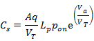
· Diffusion (storage) capacitance exist only in forward bias. · It is the excess minority carriers stored on the other side that give rise to this capacitance; · It is also a measure of the change of area under minority carrier distribution with change in voltage · There is time delay involved in storing the charges. · It is of the order of 10-9 Farad.
·
|
|
Short Base Diode |
|
Base of a
diode is the region with weaker doping.. In
Short Base
·
·
·
|
|
Switching characteristics of short base diode |
|
Turn-on time of P+N long base diode = lifetime of holes in the N legion Turn-on time of P+N short base diode= transition time of holes in the N region |
|
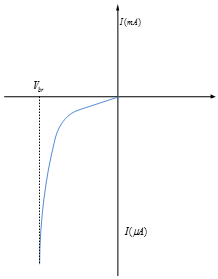
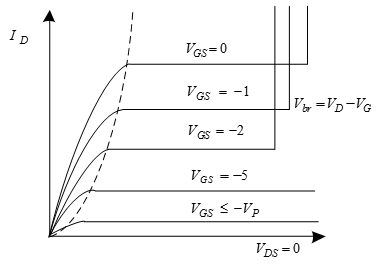
Diode Characteristics Curve |
|
|
|
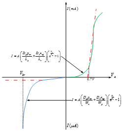
Avalanche Breakdown |
Avalanche breakdown occurs due to impact ionization of atoms by electrons that have acquired high energy from the high electric field in the depletion region.
·
Total
reverse current get multiplied by multiplication factor
· The critical electric field which can cause this breakdown is
· The breakdown voltage is given by
|
|
|
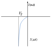
Zener breakdown |
Zener breakdown occurs due to tunneling.
Tunneling occurs if the valence band of P is directly opposite to an empty conduction band of N. This kind of alignment happens if the depletion width is very small. |
|

|
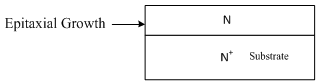
Epitaxial Growth |
|
|
|
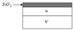
Oxidation |
|
|
|
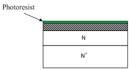
Addition of Photoresist |
|
|
|
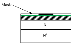
Placement of mask |
|
|
|
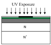
Exposure to UV |
|
|
|
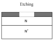
Etching |
|
|
|
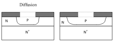
Diffusion |
|
|
|
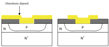
Metal Contacts |
|
|
|
|
|
|
|
|
|
|
|
![]()
![]()
![]()
|
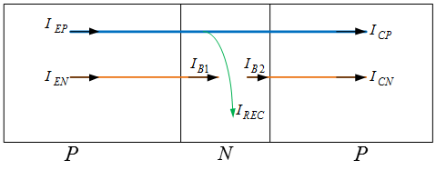
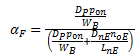
Injection Efficiency |
|
|
|
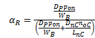
Transport Factor |
|
|
|
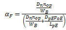
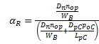
DC common base current gain |
|
|
|
DC common emitter current gain |
|
|
|
Collector current |
|
|
|
|
PNP |
NPN |
|
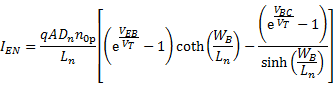
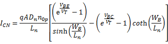
Currents Equation |
|
|
|
Ebers-Moll Equation (for PNP and NPN) |
*subscript F and R stands for active and inverse-active mode of operation respectively |
*subscript F and R stands for active and inverse-active mode of operation respectively |
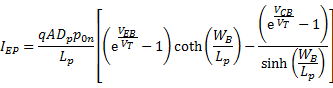
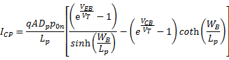
Eber Moll model for pnp BJT Transistor
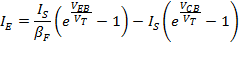
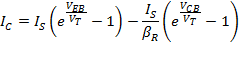
Eber Moll model for pnp BJT Transistor expressed in matrix A=BC form
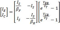


Though Eber Moll model is simple but it is not very accurate. In circuit simulation Gummel-Pool model is used
|
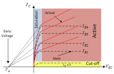
Early Effect |
PNP |
The difference
between the actual and ideal curves is because of the following: 1.
2.
3. This increases the gradient of holes in the base. 4. Consequently collector current increases.
Base width modulation is also known as Early effect. |
|
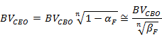
Avalanche Breakdown |
PNP |
M= avalanche multiplication factor. |
|
Punch-through |
Punchthrough occurs when the reverse bias base-collector depletion region reaches the emitter-base junction.
Generally punchthrough happens after avalanche breakdown. But if base width is very small punchthrough may precede avalanche breakdown.
In punchthrough base looses its current controlling property and collector current increases rapidly and is limited only by the external circuit resistance. |
|
|
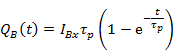
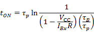
Charge Control Equation |
|
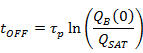
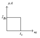
Charge control equation is a tool for calculating turn-ON and turn-OFF time of transistors. |
|
Solution of charge control equation |
|
|
|
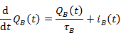
Turn-ON Time |
|
|
|
Turn-OFF Time |
|
|
|
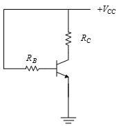
Fixed Bias |
|
|
|
|
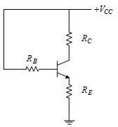
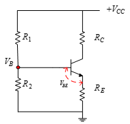
Emitter Bias |
|
|
|
|
Voltage Divider Bias |
|
|
|
|
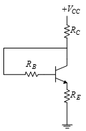
Collector Feedback Bias |
|
|
|
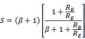
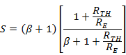
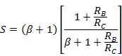
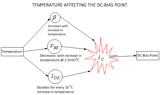
·
Stability Factor S is the rate of change of collector current ![]() with respect to
with respect to ![]() or .
or .
·
It lies between unity and infinity. S=1 is stable and S![]() is unstable.
is unstable.
![]()
![]()
![]()
|
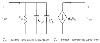
Small Signal
Model of PNP CE Transistor taking into effect the change in magnitude of only. |
|
|
||||||||||||||||||||||||
|
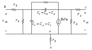
Small Signal
Model of PNP CE Transistor taking into effect the change in magnitude of |
|
|
||||||||||||||||||||||||
|
Small Signal
Model of PNP CE Transistor taking into effect the change in magnitude of |
|
|
||||||||||||||||||||||||
|
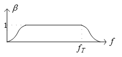
Figure of
merit
Also known as gain-bandwidth product. |
|
· It is a measure of quality of a high frequency transistor.
· If proper amplification is required at high frequency then capacitances should be small. |

|
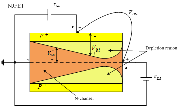
Relation between Gate source voltage and Drain source saturation voltage |
|
|
Relationship among Drain current, Drain source voltage and gate source voltage |
Valid only for
the linear region i.e.
|
|
Pinch off Voltage |
|
|
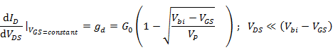
Conductance |
|
|
Channel-conductance
|
|
|
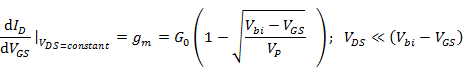
Trans-conductance
|
|
JFET properties:
|
1. Only one type of majority carrier is the cause of the current. 2. Insensitive to temperature and radiation. 3. Simple to fabricate. 4. Low noise. 5. Operates satisfactorily at high frequency. 6. Very high input impedance. 7. Low gain (compared to bipolar transistor).
|
·
Pinch-off voltage (![]() is a property of the
device.
is a property of the
device.
· It depends on physical dimension and doping densities.
|
|
Click here for video |
|
Drain to Gate Voltage |
|
To
find out region of operation compare |
|
Drain Current |
|
|
|
Breakdown voltage |
|
|
|
Threshold Voltage (also called Turn-OFF voltage |
|
It is defined
as the gate source voltage at which |
|
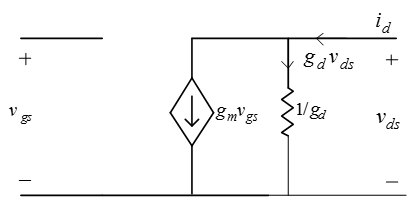
Low frequency model |
|
|
|
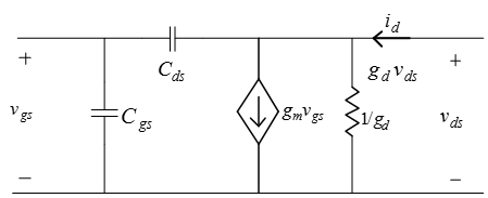
High frequency model |
|
where |
|
|
|
|
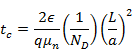
* Unity gain bandwidth.
*Capacitance is difficult to determine as it is distributed along the channel. An approximate guess about the frequency is made by taking into account total channel capacitance and total channel resistance.
![]()
![]()
![]()
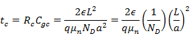
Cut
off frequency for NJFET ![]()
![]()
|
Total channel capacitance |
|
|
|
Total channel resistance |
|
|
|
RC time constant |
|
|
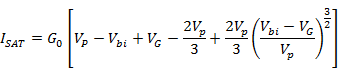
· Pinch-off voltage is the voltage at which current in JFET saturates. It is a property of the device
![]()
·
Given a JFET with ![]() defined the drain
voltage at which saturation occurs is given by (neglecting barrier potential )
defined the drain
voltage at which saturation occurs is given by (neglecting barrier potential )
![]()
·
Compare ![]() with the drain voltage
with the drain voltage ![]() .
.
·
![]() JFET is operating in LINEAR
region
JFET is operating in LINEAR
region
·
![]() JFET is operating in the
SATURATION region.
JFET is operating in the
SATURATION region.

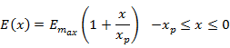
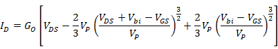
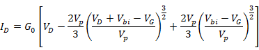
Shockley's Equation for drain current in JFET for linear region
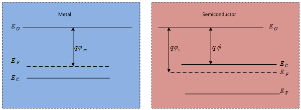
·
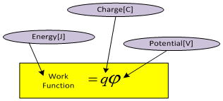
Work function (energy actually) is defined as the energy
gap between ![]()
·
![]() is the energy at vacuum.
is the energy at vacuum.
·
An electron or hole at energy![]() is said to be in a
is said to be in a ![]() free state
free state
·
Work function of metal ![]()
·
Work function of semiconductor ![]()
·
Electron affinity ![]()
|
Junction Type |
Work-function |
Type of contact ( Rectifying / Non Rectifying ) |
|
Metal-N |
|
Rectifying contact or Schottky Barrier Diode or Rectifier diode |
|
Metal-N |
|
Non-rectifying contact or Ohmic contact |
|
Metal-P |
|
Rectifying contact or Schottky Barrier Diode or Rectifier diode |
|
Metal-P |
|
Non-rectifying contact or Ohmic contact |
|
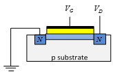
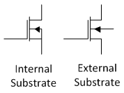
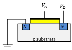
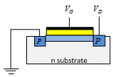
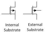
MESFET |
JFET |
|
Gate is metal. Gate-channel is a metal-semiconductor junction (Schottky diode) |
Gate is semiconductor. Gate-channel is a normal PN junction (PN diode) |
|
High-gain bandwidth product |
Low-gain bandwidth product |
|
Channel is N-GaAs in which electron mobility is few orders higher. |
Channel is semiconductor with normal electron mobility |
· Lift-off is one of the various techniques used in the fabrication of very small channel width MESFET.
|
Junction Type |
Work-function |
Type of contact |
|
Metal-N |
|
Rectifying contact or Schottky Barrier Diode or Rectifier diode |
|
Metal-N |
|
Non-rectifying contact or Ohmic contact |
|
Metal-P |
|
Rectifying contact or Schottky Barrier Diode or Rectifier diode |
|
Metal-P |
|
Non-rectifying contact or Ohmic contact |
|
Surface carrier density |
|
|
|
Current from Metal to semiconductor |
|
|
|
Current from Semiconductor to Metal |
|
|
|
Total current in MES |
|
|
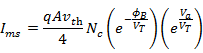
|
Schottky
barrier potential ( |
|
It is the amount of potential an electron in the metal has to overcome to cross into the semiconductor. · If it is positive, electrons can cross into semiconductor on their own. · If it is negative, electrons cannot cross into semiconductor on their own. |
|
Schottky
barrier ( |
|
It is the energy corresponding to Schottky potential. |
|
Barrier
Potential ( |
|
It is the amount of potential an electron in the semiconductor has to overcome to cross into the metal. · If it is positive, electrons can cross into metal on their own. · If it is negative, electrons cannot cross into metal on their own. |
|
Schottky Diode
|
PN Diode
|
|
High current at low voltages. (E.g.: 0.28mA at 0.4 V) |
Same current at a higher voltage (E.g.: 0.28mA at 0.6 V)
|
|
High reverse saturation current (4 orders of magnitude greater than normal) |
Low reverse saturation current |
|
Current only due to majority carriers |
Current due to both majority and minority carriers |
|
No storage capacitance hence very small turn- off time |
Turnoff time is not so small due to storage capacitance |
|
Characteristic curves |
|
|
|
Depletion Type |
Enhancement Type |
|
n-MOS |
|
|
|
p-MOS |
|
|

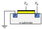

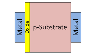
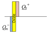
Metal Oxide semiconductor junctions have some special properties. When voltage is applied to metal-oxide-semiconductor charges accumulate on either side of the oxide.
· On the metal-oxide side charge appears on the surface.
· On the semiconductor-oxide side charges appear inside semiconductor along the boundary with the oxide.
· The density of charges accumulating on the semiconductor-oxide junction depends on the intensity and type of bias applied to the metal.
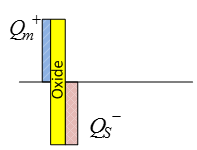
Let us consider a metal-oxide-P semiconductor junction.
1. For a negative bias the charge accumulating on the semiconductor-oxide junction is positive. This is called accumulation
2. For a positive bias the charge accumulating on the semiconductor-oxide junction is negative. This is called depletion
3. For an even more positive bias the charge accumulating on the semiconductor-oxide junction is negative. This is called inversion.
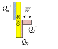
4. Increasing the bias even further increases the density of electrons beyond the density of acceptor ions. This is called strong inversion.
5. At strong inversion a depletion region of negative acceptor ions is formed just next to the inversion layer. The rest of the semiconductor is neutral.
|
Surface
carrier density |
|
|
|
Width of the
depleted region |
|
|
|
Maximum width of the depletion region |
|
|
|
Charge density
|
|
|
|
Maximum charge
density |
|
|
|
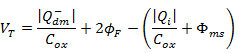
Threshold Voltage |
|
|
|
Gate voltage |
|
|
|
Oxide voltage |
|
|


|
Modes of operation |
|
|
|
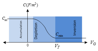
Accumulation |
|
|
|
Depletion |
|
|
|
Inversion |
|
|
|
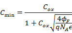
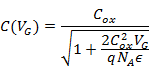
Capacitance-Voltage Measurement Graph |
|
|
Capacitance in
the inversion |
|
|
Capacitance in
the depletion |
|
|
Capacitance in
the accumulation |
|